In the early days, Apple's designs were based primarily on off-the-shelf common semiconductor devices. With the Apple II, the majority of the machine was constructed purely with standard logic. The only custom ICs (Integrated Circuits) in this design were the ROMs (Read Only Memory), being the system firmware and character ROM. This makes cloning or capturing the system in an FPGA a relatively straightforward task.
However, later Apple systems began to use ASICs and PROMS (Programmable Read Only Memory) to achieve lower device count and greater functionality in the same footprint and power budget. These optimised circuits quickly became a key part of the designs. The ASIC enables specific circuitry to be placed into a single IC and perform the task of what would normally be many ICs - in this case, over a hundred or so devices - which are replaced with just two. The Apple IIe, IIc, IIgs and the III all use ASICs as part of their design. Although these devices are detailed in the schematics, their behaviour is not as well documented. Apple did make available these prototype IOU and MMU photos, detailing the discreet logic used to create the device's internal functionality. The IOU and MMU are on the left. The Apple IIe logic board devices are on the right. The two 40-way ribbon cables simulate how the devices would interconnect to the proposed IIe motherboard as if they were in their final DIP packaging.
In order to move an Apple II design into the FPGA domain, these devices need to be understood and described. They are then defined in schematic, Verilog, or VHDL. Other methods, such as C-to-Hardware are also available, but to date are not as widely used. Once defined and written, the ASIC's functionality can be placed inside an FPGA where it interacts with the rest of the system, as it would in the original design.
ASICs also served another important purpose, and that is platform protection. The original Apple II, released in 1977, was vulnerable to being copied easily due to the lack of ASICs, as Apple discovered. After a year or so on the market, the Apple II was cloned en mass. More than 50 cloned Apple II compatible models had been produced in several different countries by the mid 1980's. It was the Brazilian outfit Unitron who spearheaded the charge, and who were eventually cloned themselves by a Taiwanese outfit after Apple had shut down the Brazilian HQ, as most copies were illegal. However several companies did managed to circumvent what was defined at the time as a "copy" in order to make legal Apple clones, (such as Franklin Computer Corp). Other companies such as Vtech embedded their Apple copies inside their own ASICs, hiding any evidence of a direct copy. Either way, Apple soon understood prevention was better than cure. When the Apple III arrived in 1980, it sported several new ASICs as part of its design and an array of logic process PROMs (or LUT - Look Up Table). Although the Apple III was an elegant and effective design academically, it was it's reliability that in the end caused this machine to become a market failure; Apple's first market failure.
In 1983 Apple released the Apple IIe. This design incorporated some of the same ASIC designs used in the Apple III, such as the keyboard controller. It also included several new ASICs that encapsulated some of the functionality of the Apple III to suit the new IIe design, such as the memory management design, which became the MMU (Memory Management Unit). This time the IIe was a success for Apple, so much so it was one of Apple's greatest offerings to the market, lasting a sales span of 11 years. Unlike the II, the IIe didn't suffer the plethora of clones. A few clones were made, but only by companies with advanced engineer resources, and only after many years of the IIe being on the market.
As a result, for the FPGA designer, gaining access to the ASICs behaviour is usually a very difficult task. However, for those determined, there are several methods that are common when reverse engineering an ASIC:
1. Documentation
After the Apple II was cloned in 1980 by Franklin Computer, Apple began to restrict information regarding its new systems. The IIe did ship with hand drawn schematics and timing diagrams, but this information was very limited in comparison to the information required to implement the ASIC device. The problem with documentation lies in the errors, how information could be interpreted, and typical changes after the documents have gone to print. However, with enough information, this approach does allow an FPGA replacement ASIC to be created, but usually involves a lot of debugging.
2. Inside Information
If many years have passed, or the design falls outside it's copyright, then inside information can leak into the public domain. For the reverse engineer, this is the easiest way of implementing the ASIC in an FPGA.
3. Hard Core Silicon
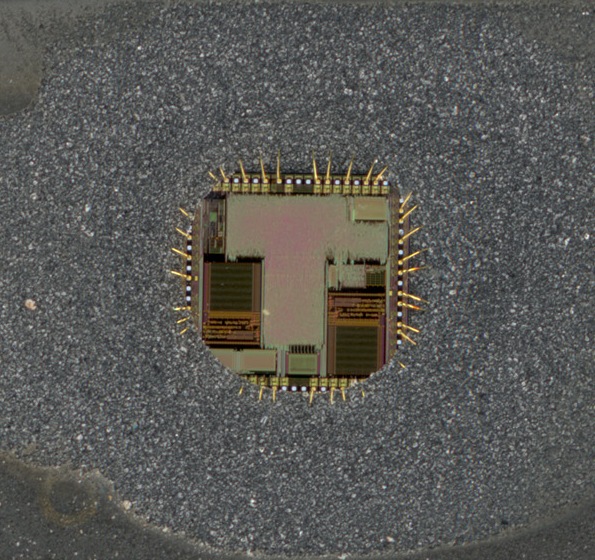
This method was commonly used to copy the ASICs in the 1980's, which involved decapping the device to gain topological access. The complex process is commonly referred to as a "Construction Analysis". Once visible, the die is then inspected, illuminated by an electron microscope and/or x-ray to gain visual access to the mask and layers to identify patterns and map the device manually. Although this is a long and painstaking process, it would seem this approach of "silicon reading" is quite common to some companies. Other companies such as Nisene Technology Group manufacture equipment exclusively for the IC reverse engineering market. With ASICs of the 80's being of a lot lower density, the task would not have been anywhere near as daunting as if you were to consider using the same techniques on a modern ASIC today.
4. Discovery
Using a board such as the PB04 to "discover" (also known as "brute force") the device's behaviour and registers. This approach is very blind, and some initial information is needed to begin, such as pin definitions and clocking. The real enabler for re-creating an ASIC using this technique is the skill and determination of the engineer researching the device. It may also take months of testing a soft ASIC side by side with the real ASIC in the development system simultaneously to fully define and produce an exact copy.


